| Sign In | Join Free | My carsrow.com |
|
| Sign In | Join Free | My carsrow.com |
|
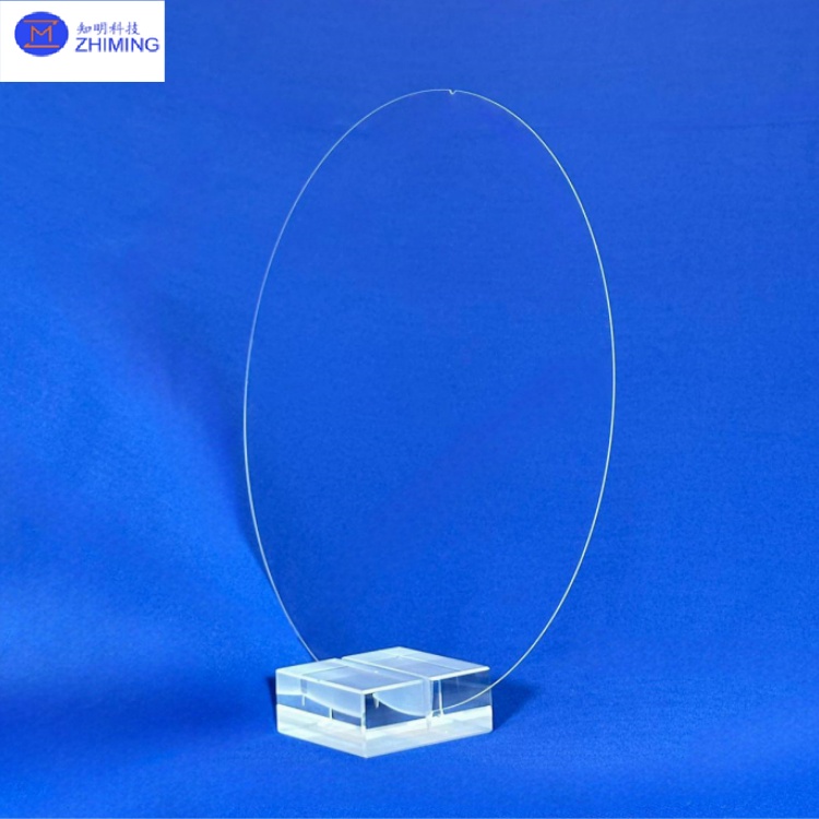
| Categories | Fused Quartz Plate |
|---|---|
| Brand Name: | ZMSH |
| Model Number: | 4 Inch Quartz Wafer |
| Certification: | rohs |
| Place of Origin: | CHINA |
| MOQ: | 10 |
| Price: | by case |
| Payment Terms: | T/T |
| Supply Ability: | 1000pcs per month |
| Delivery Time: | 5-8weeks |
| Packaging Details: | Package in 100-grade cleaning room |
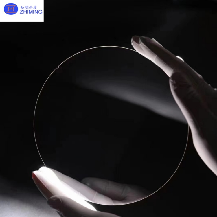
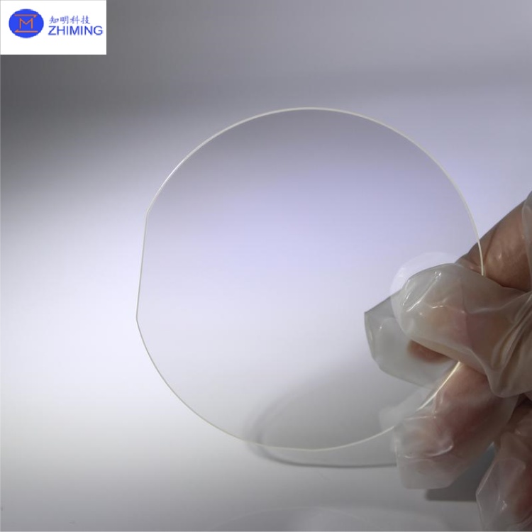
| Diameter: | 4 inch (100mm) |
| Thickness Range: | 0.5mm~1.5mm |
| Surface Roughness (Polished): | ≤0.5nm |
| Transmittance @193nm: | >93% |
| CTE (20-300°C): | 0.55×10⁻⁶/°C |
| Parallelism: | ≤3μm |
| Company Info. |
| SHANGHAI FAMOUS TRADE CO.,LTD |
| Verified Supplier |
| View Contact Details |
| Product List |
ZMSH specializes in precision-manufactured 4-inch quartz wafers, catering to high-performance optoelectronic, semiconductor, and MEMS applications. Unlike smaller formats, 4-inch quartz wafers provide extended surface area for multi-layer integration, enabling scalable production of advanced devices. Key features include:
1. Material: High-purity fused silica (SiO₂) with <50 ppm hydroxyl (OH⁻) content and <0.1 ppm metallic impurities, ensuring ultra-low optical loss .
2. Dimensions: Custom diameters (100.00 mm ±0.25 mm) and thicknesses (0.525–1.200 mm, TTV ≤10 μm) .
3. Shapes: Circular, square, or irregular geometries with non-standard apertures, stepped edges, or gradient thickness.
4. Surface Finish: Ultra-smooth surfaces (Ra ≤1.0 nm) for minimal light scattering .
| Parameter | Specification |
| Diameter | 100.00 mm ±0.25 mm |
| Thickness Range | 0.525–1.200 mm |
| Total Thickness Variation (TTV) | ≤10 μm (300 mm diameter) 4 |
| Surface Roughness (Ra) | ≤1.0 nm |
| Ultraviolet Transmittance | >92% @185–3500 nm 1 |
| Thermal Expansion Coefficient (CTE) | 0.55×10⁻⁶/°C (20–300°C) 1 |
| Resistivity (350°C) | >7×10⁷ Ω·cm |
1. Optical Superiority
Broad Spectral Transmission: >92% transmittance from 185 nm (UV) to 3500 nm (IR), ideal for UV lithography and quantum sensing .
Low Thermal Expansion: CTE of 0.55×10⁻⁶/°C (20–300°C), maintaining dimensional stability up to 1100°C .
2. Mechanical & Chemical Resilience
High Hardness: Mohs scale 7, resistant to abrasion and mechanical shock .
Acid Resistance: 30× higher durability than ceramics, suitable for aggressive chemical environments .
3. Electrical Performance
Insulation: Resistivity >7×10⁷ Ω·cm (350°C), minimizing parasitic capacitance in high-frequency circuits .
SAW Compatibility: Optimized for Surface Acoustic Wave (SAW) filters with precise cutting angles (e.g., 34.33° for FC-cut) .
1. Advanced MEMS Devices
Pressure sensors, gyroscopes, and inkjet printheads leveraging 4-inch wafers for multi-layer integration and thermal stability .
2. Optoelectronic Systems
UV laser diodes, fiber-optic collimators, and LiDAR components requiring low-loss optical paths .
3. Semiconductor Packaging
Wafer-level packaging (WLP) substrates for CMOS image sensors and RFICs, supporting TSV (Through-Silicon Via) technology .
4. Quantum Technologies
Substrates for diamond nitrogen-vacancy (NV) centers and superconducting qubits, benefiting from ultra-low defect density .
We offer full-scale customization for 4-inch quartz wafers, including:
1. Precision Machining: CNC diamond turning for <1 μm dimensional accuracy.
2. Surface Treatments: AR coatings (<0.5% reflection), hydrophobic films (water contact angle >150°).
3. Rapid Prototyping: 5–7 days for samples, supporting hybrid geometries (e.g., through-holes + notches).
1. Q: Why use 4-inch quartz wafers?
A: 4-inch quartz wafers offer a balance of cost-effectiveness and precision, ideal for MEMS sensors, optical filters, and semiconductor packaging with customizable thickness (0.5–1.5 mm) and ultra-low surface roughness (Ra ≤0.5 nm).
2. Q: What industries use 4-inch quartz wafers?
A: They are critical in MEMS devices, fiber-optic systems, and advanced semiconductor manufacturing, leveraging high-purity fused silica and exceptional thermal stability (CTE 0.55×10⁻⁶/°C).
Tag: #3 Inch Quartz Substrate, #Customized, #Fused Silica Plates, #SiO₂ Crystal, #Quartz wafers, #JGS1/JGS2 Grade, # High-Purity, #Fused Silica Optical Components, #Quartz Glass Plate, #Custom-Shaped Through-Holes, #4Inch Quartz Wafer, #Diameter 100mm, #Semiconductor Manufacturing, #Thickness Range 0.5 mm to 1.5 mm, #Ra ≤ 0.5 nm

|
