| Sign In | Join Free | My carsrow.com |
|
| Sign In | Join Free | My carsrow.com |
|
| Categories | Piezoelectric Wafer |
|---|---|
| Brand Name: | BonTek |
| Model Number: | LNOI Wafer |
| Certification: | ISO:9001, ISO:14001 |
| Place of Origin: | China |
| MOQ: | 25 pcs |
| Price: | $2000/pc |
| Payment Terms: | T/T |
| Supply Ability: | 1000 pcs/Month |
| Delivery Time: | 1-4 weeks |
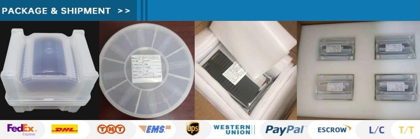
| Packaging Details: | Cassette/ Jar package, vaccum sealed |
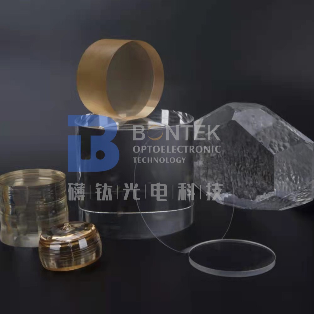
| Product: | Piezo On Insulation |
| Diameter: | 4 inch, 6 inch |
| Top Layer: | Lithium Niobate |
| Top Thickness: | 300~600nm |
| Insolation: | SiO2 Thermal Oxide |
| Insolation Thickness: | 2000±15nm; 3000±50nm; 4700±100nm |
| Substrate: | Silicon |
| Application: | Optical Waveguides and Microwaveguides |
| Company Info. |
| Hangzhou Freqcontrol Electronic Technology Ltd. |
| Verified Supplier |
| View Contact Details |
| Product List |
Enabling High-Speed Modulation And Wide Bandwidth With LNOI POI
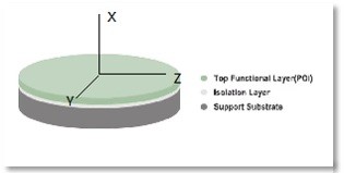
Piezo on Insulation (POI) refers to a technology where piezoelectric materials are integrated onto an insulating substrate. This allows for the utilization of the piezoelectric effect while providing electrical isolation. The POI technology enables the development of various devices and systems that harness the unique properties of piezoelectric materials for sensing, actuation, and energy harvesting applications.
POI (Piezo on Insulation) technology finds various applications in different fields due to its ability to combine the advantages of piezoelectric materials with electrical isolation. Such as sensors, Microelectromechanical Systems and Energy Storage and Generation.
The versatility of integrating piezoelectric materials onto an insulating substrate opens up possibilities for innovative solutions in diverse fields, including electronics, energy, healthcare, and more.
| LNOI Wafer | |||
| Structure | LN / SiO2 / Si | LTV / PLTV | < 1.5 μm ( 5∗ 5 mm2 ) / 95% |
| Diameter | Φ100 ± 0.2 mm | Edge Exclution | 5 mm |
| Thickness | 500 ± 20 μm | Bow | Within 50 μm |
| Primary Flat Length | 47.5 ± 2 mm 57.5 ± 2 mm | Edge Trimming | 2 ± 0.5 mm |
| Wafer Beveling | R Type | Environmental | Rohs 2.0 |
| Top LN Layer | |||
| Average Thickness | 400/600±10 nm | Uniformity | < 40nm @17 Points |
| Refraction index | no > 2.2800, ne < 2.2100 @ 633 nm | Orientation | X axis ± 0.3° |
| Grade | Optical | Surface Ra | < 0.5 nm |
| Defects | >1mm None; ≦1 mm Within 300 total | Delamination | None |
| Scratch | >1cm None; ≦1cm Within 3 | Primary Flat | Perpendicular to +Y Axis ± 1° |
| Isolation SiO2 Layer | |||
| Average Thickness | 2000nm ± 15nm 3000nm ± 50nm 4700nm ± 100nm | Uniformity | < ±1% @17 Points |
| Fab. Method | Thermal Oxide | Refraction index | 1.45-1.47 @ 633 nm |
| Substrate | |||
| Material | Si | Orientation | <100> ± 1° |
| Primary Flat Orientation | <110> ± 1° | Resistivity | > 10 kΩ·cm |
| Backside Contamination | No visible stain | Backside | Etch |


|
