| Sign In | Join Free | My carsrow.com |
|
| Sign In | Join Free | My carsrow.com |
|
| Categories | Technical Ceramic Parts |
|---|---|
| Brand Name: | ZG |
| Model Number: | MS |
| Certification: | CE |
| Place of Origin: | CHINA |
| MOQ: | 1 piece |
| Price: | USD10/piece |
| Payment Terms: | L/C, D/A, D/P, T/T, Western Union, MoneyGram |
| Supply Ability: | 10000 pieces per month |
| Delivery Time: | 3 working days |
| Packaging Details: | Strong wooden box for Global shipping |
| Application: | red , yellow , and green LED ( light-emitting diodes ) |
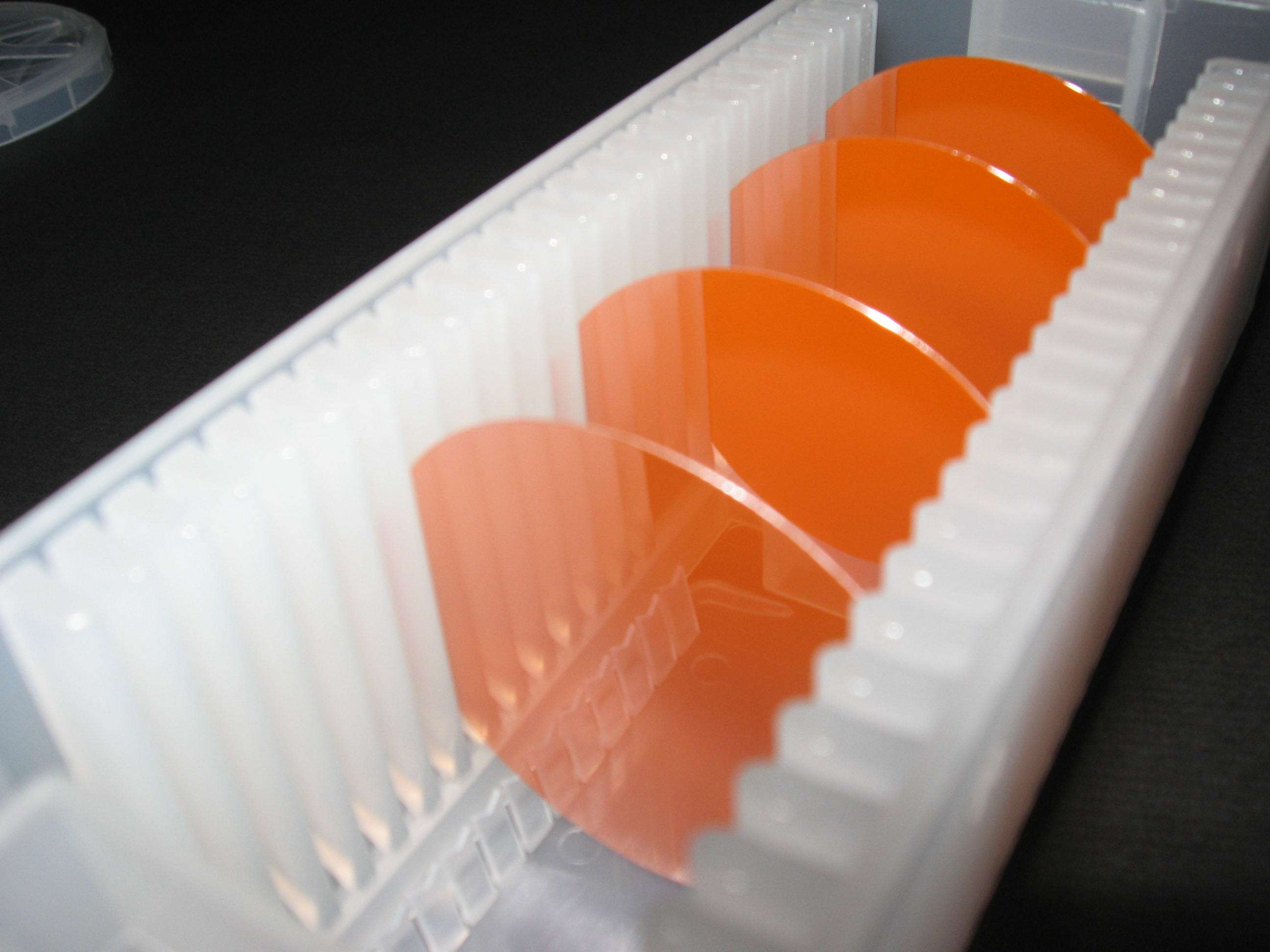
| Diameter: | Ø 2" |
| Thickness: | 400 um |
| Grade: | Epi polished grade / mechanical grade |
| Company Info. |
| HENAN ZG INDUSTRIAL PRODUCTS CO.,LTD |
| Verified Supplier |
| View Contact Details |
| Product List |
Single Crystal GaP Wafer ( Gallium Phosphide ),widely used as red , yellow , and green LED ( light-emitting diodes )
We provides high quality single crystal GaP wafer ( Gallium phosphide ) to electronic and optoelectronic industry in diameter up to 2 inch . Gallium phosphide ( GaP ) crystal is an orange-yellow semi-translucent material formed by two elements , Gallium and Phosphide , growth by Liquid Encapsulated Czochralski ( LEC ) method . GaP wafer is an important semiconductor material which have unique electrical properties as other III-V compound materials and is widely used as red , yellow , and green LED ( light-emitting diodes ) . We have as-cut single crystal GaP wafer for your LPE application , and also provide epi ready grade GaP wafer for your MOCVD & MBE epitaxial application . Please contact us for more product information .
III-V Compound Wafer
We provides a wide range of compound wafer including GaAs wafer, GaP wafer, GaSb wafer, InAs wafer, and InP wafer .
Electrical and Doping Specification
| Dopant available | S / Zn / Cr / Undoped |
|---|---|
| Type of conductivity | N / P ,Semi-conducting / Semi-insulating |
| Concentration | 1E17 - 2E18 cm-3 |
| Mobility | > 100 cm2 / v.s. |
Product Specification
| Growth | LEC |
|---|---|
| Diameter | Ø 2" |
| Thickness | 400 um |
| Orientation | <100> / <111> / <110> or others |
| Off orientation | Off 2° to 10° |
| Surface | One side polished or two sides polished |
| Flat options | EJ or SEMI. Std . |
| TTV | <= 10 um |
| EPD | <= 2E5 cm-2 |
| Grade | Epi polished grade / mechanical grade |
| Package | Single wafer container |

|
