| Sign In | Join Free | My carsrow.com |
|
| Sign In | Join Free | My carsrow.com |
|
| Categories | HDI PCB |
|---|---|
| Brand Name: | TOPCBS |
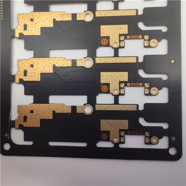
| Model Number: | 0.95mm Anylayer HDI / 12L mainboard |
| Certification: | UL94V0 |
| Place of Origin: | Suzhou China |
| MOQ: | Negotiation |
| Price: | Negotiation |
| Payment Terms: | T/T |
| Supply Ability: | 10000unit per month |
| Delivery Time: | 10-14working days |
| Packaging Details: | 20unit per package package size:20*15*10cm |
| PCB Standard:: | IPC-6012, UL, ISO9001 |
| Service type: | PCB Prototype |
| Raw material: | EM370(D) |
| Layer count: | 12Layer |
| Board Thickness: | 0.95mm |
| Stack up: | Anylayer |
| Finish treatment: | Immersion gold+OSP |
| Line width/space: | 50um / 60um |
HDI Fourteen Layer First-Order Board PCB and Four Layer Power Board PCB
. 1 to 36-layer rigid and 2-to 14-layer flex and rigid flex PCBs
. Blind/buried vias with sequential lamination
. HDI build up micro via technology with solid copper filled vias
. Via in pad technology with conductive and non-conductive filled
vias
. Heavy-copper up to 12oz.Board thickness up to 6.5mm.Board size up
to 1010X610mm.
. Special materials and hybrid construction
Specifications:
| Name | 0.95mm Anylayer HDI / 12L mainboard |
| Number of Layers | 12 |
| Quality Grade | IPC 6012 Class 2,IPC 6012 Class 3 |
| Material | EM370(D) |
| Thickness | 0.95mm |
| Min Track/Spacing | 50um/60um |
| Min Hole Size | Laser 75um; Drilling size 200um |
| Solder Mask | Blue |
| Silkscreen | White |
| Surface Finish | Immersion gold,OSP |
| Finished Copper | 12um |
| Production time | 10-21 working days |
| Lead time | 2-3 days |
3. Advantages:
The most common reason for using HDI technology is a significant increase in packaging density. The space obtained by finer track structures is available for components. Besides, overall space requirements are reduced will result in smaller board sizes and fewer layers.
Usually FPGA or BGA are available with 1mm or less spacing. HDI technology makes routing and connection easy, especially when routing between pins.


|