| Sign In | Join Free | My carsrow.com |
|
| Sign In | Join Free | My carsrow.com |
|
| Categories | GPON OLT SFP |
|---|---|
| Brand Name: | HiOSO |
| Model Number: | C+++ |
| Certification: | CCC,Rohs, CE |
| Place of Origin: | China |
| MOQ: | 1000 PCS |
| Price: | Negotiable |
| Payment Terms: | T/T, Western Union, MoneyGram, D/P |
| Supply Ability: | 10000pcs/month |
| Delivery Time: | 5-10working days |
| Packaging Details: | Standard Carton Packing |
| Type: | GPON OLT SFP C+++ |
| Operation case temperature: | 0~70°C or -40~85°C |
| Standard: | Comply with ITU-T G984.2 Amendment 1 |
| Name: | SFP with SC/PC Connector Transceiver |
| Company Info. |
| HiOSO Technology Co., Ltd. |
| View Contact Details |
| Product List |
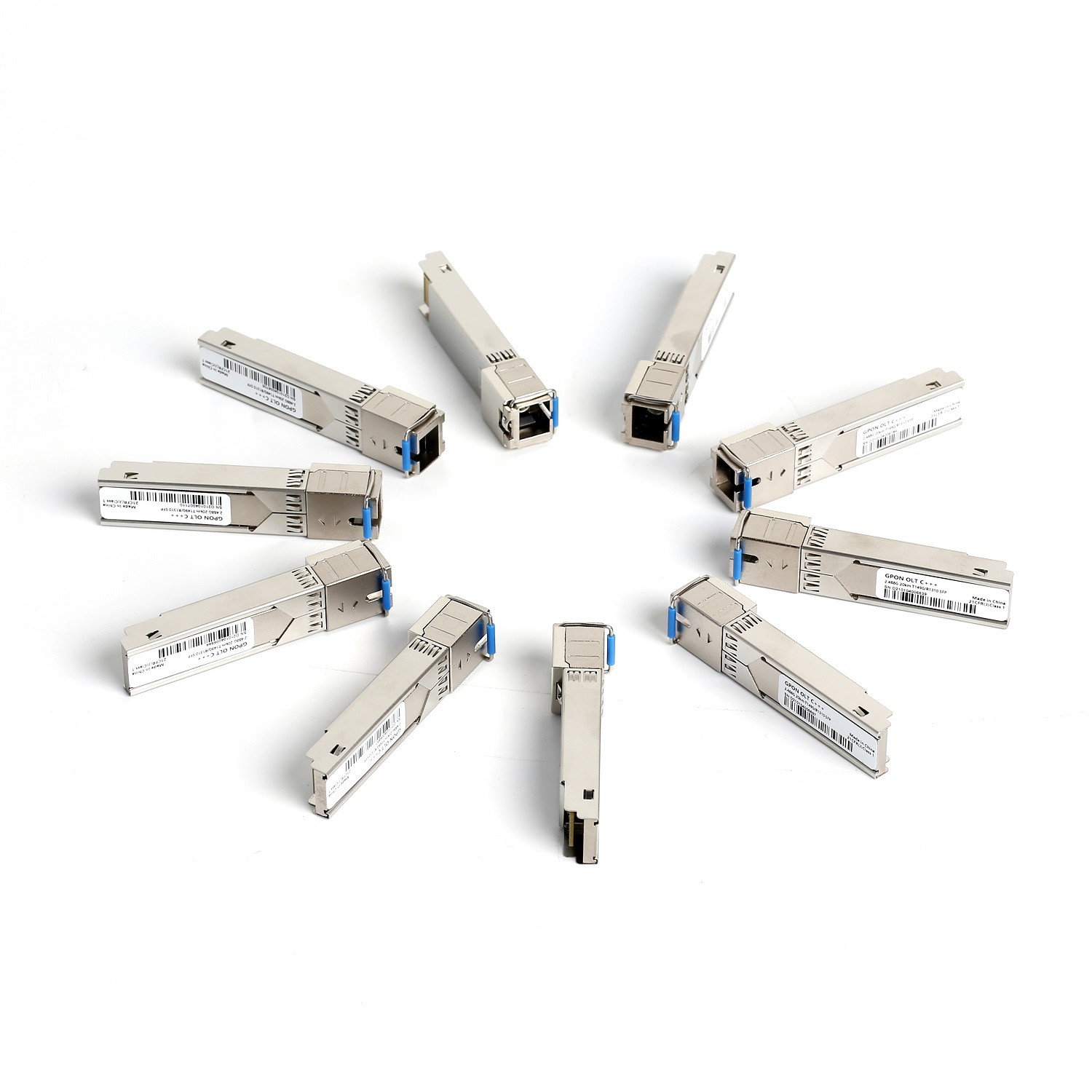
![]() GPON Class C+++ SFP OLT Transceiver
GPON Class C+++ SFP OLT Transceiver
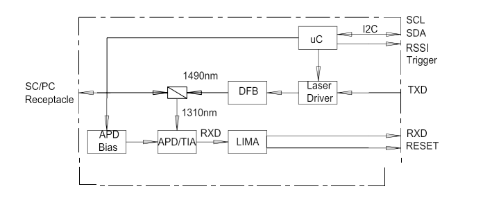
l 1490 nm DFB Tx with isolator
l 1310 nm APD Rx
l Digital diagnostics SFF-8472 Compliant
l 2488 Mbps continuous mode Transmission
l 1244 Mbps Burst mode receiver Data Rate
l RX Fast Burst Mode Detection
l Provide fast RSSI function
l Operation case temperature: 0~70°C or -40~85°C
l Class C+++ link budget
l Comply with ITU-T G984.2 Amendment 1
l Complies with RoHS directive (2002/95/EC)
2. Application
l GPON OLT Class C+++
l FTTx
3. Function Diagram
4. Recommended Operating Conditions
| Parameter | Symbol | Min. | Max. | Unit | Notes |
| Storage Temperature | TSTG | -40 | 85 | °C | |
| Operating Case Temperature | TC | 0 | 70 | °C | ZP5432043-QCS |
| Operating Case Temperature | TC | 0 | 70 | °C | ZP5432043-QIS |
| Power Supply Voltage | VCC | 3.1 | 3.5 | V | |
| Total Power Supply Current | Icc | - | 500 | mA |
5. Transmitter Characteristics
| Parameter | Symbol | Min. | Typ. | Max. | Units | Notes |
| Optical Transmitter Power | P0 | 7 | - | 11 | dBm | 1 |
| Optical Transmitter Power off | POFF | - | - | -39 | dBm | |
| Output Center Wavelength | λ | 1480 | - | 1500 | nm | |
| Output Spectrum Width | Δλ | - | - | 1.0 | nm | |
| Side Mode Suppression Ratio | SMSR | 30 | - | - | dB | |
| Extinction Ratio | ER | 9 | - | - | dB | |
| Optical Rise Time | - | - | - | 160 | ps | |
| Optical Fall Time | - | - | - | 160 | ps | |
| Optical Eye Diagram | Compliant with ITU-T G.984.2 Mask | |||||
| Tolerence to Tx Back Reflection | - | -15 | - | - | dB | |
| Data Rate | - | - | 2.488 | - | Gb/s | |
| Differential Input Voltage | VPP | 300 | - | 1200 | mV | |
| Differential Input Impedance | ZIN | 80 | 100 | 120 | ohm | |
| Tx_fault Output Voltage- High | VIH | 2.4 | - | - | V | |
| Tx_fault Output Voltage- Low | VIL | - | - | 0.4 | V | |
| Tx_Dis Input Voltage- High | VIH | 2.0 | - | - | V | |
| Tx_Dis Input Voltage- Low | VIL | - | - | 0.8 | V | |
Note 1: 2.488Gbps continuous-mode , PRBS223-1.
6. Receiver Characteristics
| Parameter | Symbol | Min. | Typ. | Max. | Units | Notes |
| Wavelength of Operation | - | 1260 | - | 1360 | nm | - |
| Data Rate | - | - | 1.244 | - | Gb/s | - |
| Sensitivity | Sen | - | - | -32 | dBm | 1 |
| Saturation Optical Power | Sat | -8 | - | - | dBm | 1 |
| Burst Packet Detect sensitivity | - | - | - | -32 | dBm | 1 |
| Receiver Reflectance | - | - | - | -12 | dB | |
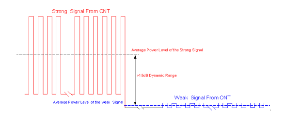
| Receiver Burst-mode Dynamic Range | - | 15 | - | - | dB | 2 |
| Data Output Differential Swing | - | 400 | - | 1600 | mV | |
| RSSI accuracy | - | -3 | - | 3 | dB | 3 |
| BPD Output Voltage- High | VIH | 2.4 | - | - | V | 4 |
| BPD Output Voltage- Low | VIL | - | - | 0.4 | V | 4 |
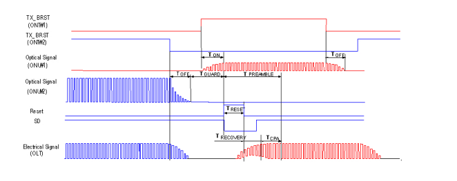
| Guard Time | TGUARD | - | 32 | - | bits | - |
| Rest Width | TRESET | 16 | - | bits | ||
| Reset-Low | 0 | 0.8 | V | |||
| Reset-High | 2.0 | Vcc | V | |||
| Receiver Amplitude Recovery Time | TRECOVERY | - | 24 | 32 | bits | |
| Signal Detect De-Asset Time | 12.8 | ns | ||||
| Signal Detect Assert Time | 50 | ns | ||||
| Optical Signal During Time | TONT EN_DUR | 300 | - | - | ns | 5 |
| RSSI Trigger Delay | TD | 0 | - | 3000 | Ns | 6 |
| RSSI Trigger Width | TW | 300 | - | TONT EN_DUR | ns |
Note 1: Measured with 1310nm, 1.244Gbps PRBS223-1 burst-mode optical input, ER=10dB, BER=1x10⁻¹⁰; Single burst packet length is 40us and packet interval is 40us.
Note 2: Input optical power level difference of adjacent burst packets.
Note 3: Receiver optical power ranged from -8dBm to -28dBm, measured with 1310nm, 1.244Gbps PRBS27-1 burst-mode optical input, ER=10dB, 50%duty cycle.
Note 4: BPD assert low when module receive “Reset” signal, assert high when burst package is detected and latch to high state until next “Reset” signal.
Note 5: For RSSI Measurement
Note 6: Refer to first bit of the preamble
 |
8. Timing Parameter Definitions in Burst Mode Sequence
9. RSSI Timing Sequence
10. Digital Diagnostic Monitoring Accuracy
| Parameter | Accuracy | Units | Notes |
| Transceiver Temperature | ±3 | °C | Temperature sensor |
| Power Supply Voltage | ±3 | % | Vcc=3.13~3.47V |
| TX Bias Current | ±10 | mA | |
| TX Optical Power | ±3 | dB | Average Power |
| Rx Power | ±3 | dB |
11. Pin Definitions
| Pin# | Name | Function |
| 1 | VeeT | Transmitter Ground |
| 2 | TX_Fault | Transmitter Fault Indication, LVTTL Output, Active High |
3 | TX_Disable | Transmitter Disable, LVTTL Input. Optical output power is off when this PIN is high or left unconnected. |
| 4 | SDA | I2C Data |
| 5 | SCL | I2C Clock |
| 6 | MOD-DEF(0) | Internally grounded |
| 7 | Reset | Receiver Reset , LVTTL Input. Set “Reset” high at the end of previous burst, 2 bytes in duration |
| 8 | BPD | Burst Packet Detect, LVTTL output. BPD assert low when module receives “reset” signal, assert high when incoming burst is present. |
| 9 | RSSI_Trigger | RSSI Trigger Signal from Host, LVTTL input. |
| 10 | VeeR | Receiver Ground |
| 11 | VeeR | Receiver Ground |
| 12 | RD- | Inv. Received Data Out, LVPECL,DC coupled |
| 13 | RD+ | Received Data Out, LVPECL,DC coupled |
| 14 | VeeR | Receiver Ground |
| 15 | VccR | Receiver Power |
| 16 | VccT | Transmitter Power |
| 17 | VeeT | Transmitter Ground |
| 18 | TD+ | Transmit Data In, LVPECL or CML (AC coupled; internally 100 ohms differential termination) |
| 19 | TD- | Inv. Transmit Data In, LVPECL or CML (AC coupled; internally 100 ohms differential termination) |
| 20 | VeeT | Transmitter Ground |
12. ![]()
![]()
![]()
![]()
![]() Outline Drawing
Outline Drawing
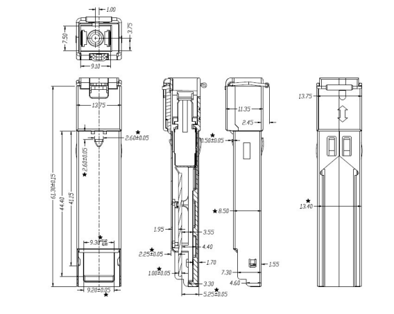
Unit:mm
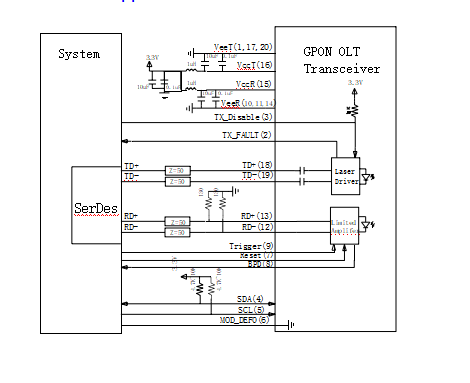
13. Recommended Application Circuit
When the ambient is reaching 85C max as declared, the internal case is hot surface please don't touch.

|
