| Sign In | Join Free | My carsrow.com |
|
| Sign In | Join Free | My carsrow.com |
|
| Categories | Gallium Nitride Wafer |
|---|---|
| Brand Name: | zmkj |
| Model Number: | GaN-non-polar |
| Place of Origin: | CHINA |
| MOQ: | 1pc |
| Price: | by case |
| Payment Terms: | L/C, T/T |
| Delivery Time: | 2-4weeks |
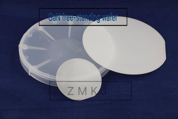
| Packaging Details: | single wafer case in 100-grade cleaning room |
| Material: | GaN single crystal |
| method: | HVPE |
| size: | 10x10mm, 5x5mm |
| thickness: | 350um |
| industry: | LD,led,laser device,detector, |
| surface: | sing or double side poliseed |
| grade: | for LD |
| type: | Non-Polar Freestanding GaN Substrates |
| Company Info. |
| SHANGHAI FAMOUS TRADE CO.,LTD |
| Verified Supplier |
| View Contact Details |
| Product List |
2inch GaN substrates template,GaN wafer for LeD,semiconducting Gallium Nitride Wafer for ld,GaN template, mocvd GaN Wafer,Free-standing GaN Substrates by Customized size,small size GaN wafer for LED, mocvd Gallium Nitride wafer 10x10mm,5x5mm, 10x5mm GaN wafer,Non-Polar Freestanding GaN Substrates(a-plane and m-plane)
GaN Wafer Characteristic
| Product | Gallium nitride (GaN) substrates | ||||||||||||||
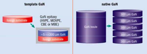
| Product Description: | Saphhire GaN template is presented Epitxial hydride vapor phase epitaxy (HVPE) method. In the HVPE process, the acid produced by the reaction GaCl, which is in turn reacted with ammonia to produce gallium nitride melt. Epitaxial GaN template is a cost-effective way to replace gallium nitride single crystal substrate. | ||||||||||||||
| Technical parameters: |
| ||||||||||||||
| Specifications: | GaN epitaxial film (C Plane), N-type, 2 "* 30 microns, sapphire; GaN epitaxial film (C Plane), N-type, 2 "* 5 microns sapphire; GaN epitaxial film (R Plane), N-type, 2 "* 5 microns sapphire; GaN epitaxial film (M Plane), N-type, 2 "* 5 microns sapphire. AL2O3 + GaN film (N-type doped Si); AL2O3 + GaN film (P-type doped Mg) Note: according to customer demand special plug orientation and size. | ||||||||||||||
| Standard Packaging: | 1000 clean room, 100 clean bag or single box packaging |
Application
GaN can be used in many areas such as LED display, High-energy
Detection and Imaging,
Laser Projection Display, Power Device, etc.
Specifications:
GaN Template specification
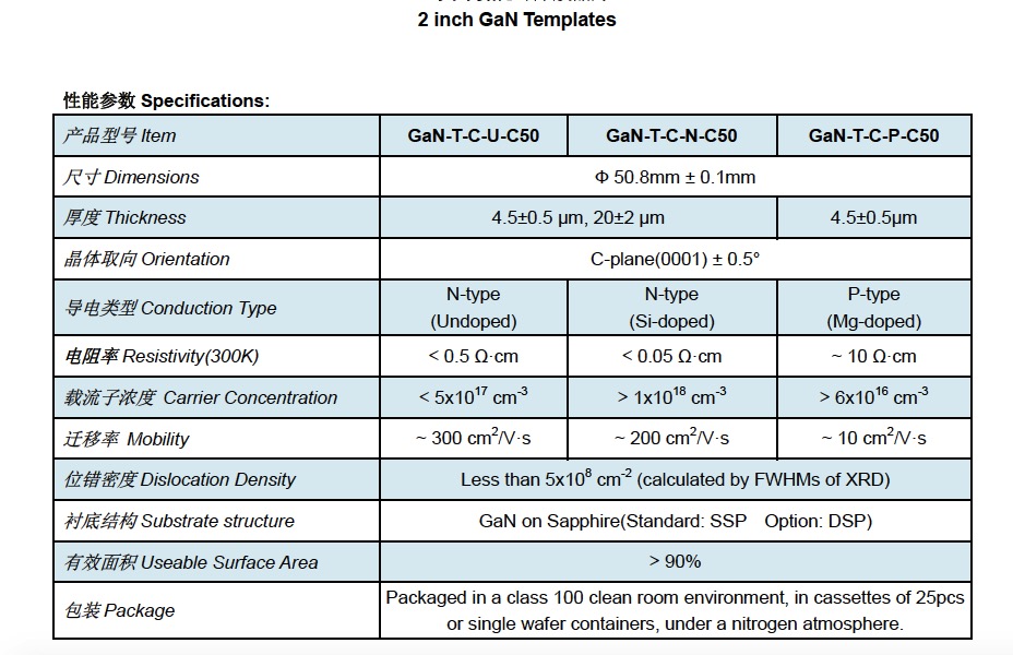
| Item | GaN-FS-C-U-C50 | GaN-FS-C-N-C50 | GaN-FS-C-SI-C50 |
| Dimensions | e 50.8 mm ± 1 mm | ||
| Thickness | 350 ± 25 pm | ||
| Useable Surface Area | > 90% | ||
| Orientation | C-plane (0001) off angle toward M-Axis 0.35° ± 0.15° | ||
| Orientation Flat | (1-100) ±0.5°, 16.0 ±1.0 mm | ||
| Secondary Orientation Flat | (11-20) ±3°, 8.0 ±1.0 mm | ||
| TTV(Total Thickness Variation) | < 15 pm | ||
| BOW | < 20 pm | ||
| Conduction Type | N-type | N-type | Semi-Insulating (Fe-doped) |
| Resistivity(3O0K) | < 0.1 Q・cm | < 0.05 Q・cm | >106 Q・cm |
| Dislocation Density | From 1x105 cm-2 to 3x106 cm-2 | ||
| Polishing | Front Surface: Ra < 0.2 nm (polished); or < 0.3 nm (polished and surface treatment for epitaxy) | ||
| Back Surface: 0.5~1.5 pm; option: 1~3 nm (fine ground); < 0.2 nm (polished) | |||
| Package | Packaged in a class 100 clean room environment, in single wafer containers, under a nitrogen atmosphere. | ||
| size | 4”GaN Substrates |
| Item | GaN-FS-N |
| Dimensions size | Ф 100.0mm ± 0.5mm |
| Thickness of Substrate | 450 ± 50 µm |
| Orientation of Substrate | C-axis(0001) toward M-axis 0.55± 0.15° |
| Polish | SSP Or DSP |
| Method | HVPE |
| BOW | <25UM |
| TTV | <20um |
| Roughness | <0.5nm |
| resistivity | 0.05ohm.cm |
| Dopant | Si |
(002) FWHM&(102) FWHM | <100arc |
Quantity and maximum size of holes and pits | Production grade ≤23@1000 um;Research grade ≤68@1000 um |
| Dummy grade ≤112@1000 um | |
| Useable area | P level>90%; R level>80%: Dlevel>70%(edge and macro defects exclusion) |
| Non-Polar Freestanding GaN Substrates(a-plane and m-plane) | ||
| Item | GaN-FS-a | GaN-FS-m |
| Dimensions | 5.0mm×5.5mm | |
| 5.0mm×10.0mm | ||
| 5.0mm×20.0mm | ||
| Customized Size | ||
| Thickness | 330 ± 25 µm | |
| Orientation | a-plane ± 1° | m-plane ± 1° |
| TTV | ≤15 µm | |
| BOW | ≤20 µm | |
| Conduction Type | N-type | |
| Resistivity(300K) | < 0.5 Ω·cm | |
| Dislocation Density | Less than 5x106 cm-2 | |
| Useable Surface Area | > 90% | |
| Polishing | Front Surface: Ra < 0.2nm. Epi-ready polished | |
| Back Surface: Fine ground | ||
| Package | Packaged in a class 100 clean room environment, in single wafer containers, under a nitrogen atmosphere. | |
2.ZMKJ provides GaN wafer to microelectronics and optoelectronics industry in diameter 2" to 4".
GaN epitaxial wafers are grown by HVPE or MOCVD method , can be used as an ideal and excellent substrate for high frequency , high speed and high power device . Currently we can offer GaN epitaxial wafer for fundamental research and device product development use, including GaN template , AlGaN
and InGaN . Besides standard GaN based wafer,you are welcome to
discuss your epi layer structure .
|
